Aarhus University Seal

Transmission & Scanning Electron Microscopy

The Interdisciplinary Nanoscience Center at Aarhus University: Transmission and scanning electron microscopy

Transmission and scanning electron microscopy

Transmission electron microscopy

The transmission electron microscope is an optical analogue to the conventional light microscope. It is based on the fact that electrons can be ascribed a wavelength (of the order of 2.5 pm) and interact with magnetic fields as a point charge. A beam of electrons is applied instead of light, and the glass lenses are replaced by magnetic lenses. The lateral resolution of the best microscopes are down to atomic resolution.

A schematic presentation of the microscope is shown in Figure1. With an electron gun an electron beam is formed, which is accelerated by an electric field formed by a voltage difference of, typically, 200 kV. By condenser lenses, the electron beam is focused to a spot of 1 mm on the thin film to be investigated. The first image, which is formed by the objective lens, is magnified typically x25. The following lenses give a final magnification of the image of more than x10^6. Additionally, to thin-sample images, electron diffraction patterns can also be formed on the final image screen. The electron rays corresponding to bright field imaging and (selected area) diffraction are shown in the left and right drawings of Figure1, respectively. In bright field imaging, the image of a thin sample is formed by the electrons that pass the film without diffraction, the diffracted electrons being stopped by a diaphragm. In the corresponding dark field imaging mode, a diffracted beam is used for imaging.

The microstructure, e.g., the grain size and lattice defects are studied by use of the image mode, while the crystalline structure is studied by the diffraction mode. Additionally, the chemical composition of small volumes, e.g., grain boundaries, can be obtained by detection of x-rays emitted from the film.

Samples of electron microscopy in form of films mounted on fine-meshed grids are required to be very thin. In case near-atomic resolution is required film thicknesses have to be limited to a few tens of Å. Therefore, the quality of the electron microscopy work is sometimes limited by the thinning-down procedure as structural changes may occur during the thinning.
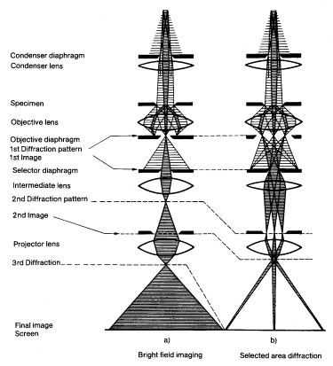
Figure1. Schematic presentation of a transmission electron microscope.

Figure1. Schematic presentation of a transmission electron microscope.

Scanning electron microscopy

A schematic representation of the scanning electron microscope, which is used to study the surfaces are studied, is shown in Figure2. The electrons are accelerated in a potential difference typically of the order of 10-20 keV, and the magnetic lenses form an electron spot of a size of a few nm. When the energetic electrons hit the surface under investigation, secondary electrons are emitted (SE), some incident electrons are being backscattered (BSE), x-rays are emitted (X) and a current is measured to the sample (SC and EBIC). A deflection coil system scans the focused electron beam in a raster across the surface. In synchronism with this is an electron beam of a separate cathode-ray tube (CRT) scanned over the screen, while the intensity of the CRT is modulated by one of the signals SE, BSE, X, or SC and EBIC to form a image of the surface.
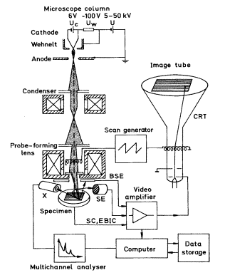
Figure2. A Schematic presentation of a scanning electron microscope.

Figure2. A Schematic presentation of a scanning electron microscope.

Cryo-electron microscopy

Several difficulties are involved in imaging small organic objects such as proteins by TEM or SEM: many organic samples may not tolerate a bombardment of electrons, or removing them from their natural surrounding may destroy them.

The technique of cryo-electron microscopy overcomes these difficulties by quick-freezing the sample in, e.g., liquid ethane at -150 degr. celsius which forms a vitreous layer of ice around the sample. This layer decreases the damages inflicted by the electrons, and because the sample is not dehydrated it will not undergo significant conformational changes when transferred to the microscope.

The downside to this technique is relatively low as neither O, H nor C contain many electrons which the inflicting electrons can interact with. This makes accurate observations relatively difficult compared to observations of samples prepared by, e.g., electronegative staining.