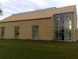
The Nanofabrication Facility building is a modern class 100 (ISO class 5) cleanroom built in 2008. The common facility services users from the Faculty of Natural Sciences and Faculty of Technical Sciences, which includes the Departments of Engineering, Molecular Biology, Chemistry, Physics and Astronomy, and the iNANO center. Examples of activities are:
The facility is equipped with state-of-the-art instruments for nanofabrication. We have equipment for making nano and micropatterns such as electron beam lithography, photolithography, and nanoimprint lithography. These instruments allow us to make patterns between 10 nm to 100 mm. The patterns can be then transferred into thin-films of metals, insulators and conductors using deep reactive ion etching and physical vapor deposition. Examples of thin-film materials are gold, titanium, chromium, silicon, silicon dioxide, and silicon nitride. We also work with materials such as graphene and tin sulphide for solar cell applications. Typically, the thickness of these thin-films is between 10 nm to 1000 nm. For analysis of micro and nanostructures, the facility includes a range of characterization instruments such as atomic force microscopy, scanning electron microscopy, ellipsometry, and electrical characterization.