The solid-liquid interface approximating the Schottky junction model for 2D material does not fully explain the efficient charge transfer during the reaction. Meanwhile, from an electronic point of view, the charge transfer behaviour across the interface in the reaction is also not easy to get an answer from the device, such as 2D materials-based field effect transistor.
Recently, In-situ synthesis of two-dimensional material electrocatalysts, such as single atom catalyst exhibited excellent performance on electrocatalysis due to the highly exposed single active site in phase transition process. However, the mechanism of synthetic strategy needs to be further revealed.
In this project, Electrochemical Atomic Force Microscopy (EC-AFM) allows in-situ monitoring of both the junction interface and phrase transition during redox reactions in batteries or Field Effect Transistor (FET). As a result, the relation between the electrode structure / morphology and its electrochemical activity can be established.
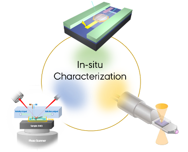
Schematic illustration of in-situ characterization in this project
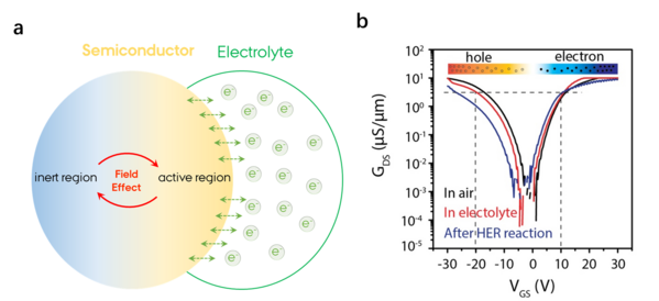
To accurately understand the carrier transport operation of the semiconductor catalyst, only the conductive signal can be completely separated from the catalytic reaction current. When a catalytic reaction occurs in a semiconductor catalyst, the surface of the catalyst is regulated by the reaction electrochemical potential. If the type of reaction is matched with the carrier of the catalytic material, the surface of the catalyst will be turned into a low-resistance state to accelerate the charge transfer; conversely, the surface will be closed to a high-resistance state to hinder the charge transfer1. molybdenum sulfide (MoS2)2 and NiFe layered double hydroxides (NiFe LDHs)3 have been recognized the most promising semiconductor catalysts for water splitting process, but still suffer from large overpotential for large-scale water splitting instruments.
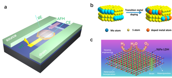
Schematic illustration FET and 2D semiconductors including MoS2 and NiFe LDHs
We are looking forward to designing a high-precision in-situ electrical/electrochemical test platform and a matching miniature electrocatalytic device to achieve simultaneous measurement of catalytic material source leakage current and electrochemical current. With this system, the effect of gate current regulation in semiconductor electrocatalysis is studied, that is, the conductivity of the surface of a semiconductor material in some specific reactions is turned on into a high-conductivity state or is turned off into insulation in other reactions4.
Advanced Science, 2020, 7(3): 1901382. https://doi.org/10.1002/advs.201901382
The catalytic behavior of nanomaterials is also controlled by the structure-activity relationship of the catalytic center and structure. We expect to use real-time monitoring of the morphology evolution of semiconductor catalysts in actual electrochemical processes using in-situ EC-AFM and Kelvin probe force microscope, KPFM. Thereby constructing the spatial-temporal correlation evolution between spectroscopy and material properties.
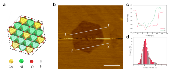
Structural and morphology analysis of NiCo LDH by KPFM
1. Song, F.; Hu, X., Exfoliation of layered double hydroxides for enhanced oxygen evolution catalysis. Nat. Commun. 2014, 5, 4477.
2. Tedstone, A. A.; Lewis, D. J.; O’Brien, P., Synthesis, properties, and applications of transition metal-doped layered transition metal dichalcogenides. Chem. Mater. 2016, 28 (7), 1965-1974.
3. Gong, M.; Dai, H., A mini review of NiFe-based materials as highly active oxygen evolution reaction electrocatalysts. Nano Res. 2015, 8 (1), 23-39.
4. He, Y.; He, Q.; Wang, L.; Zhu, C.; Golani, P.; Handoko, A. D.; Yu, X.; Gao, C.; Ding, M.; Wang, X., Self-gating in semiconductor electrocatalysis. Nat. Mater. 2019, 18 (10), 1098-1104.
3.3 Investigation of Two-dimensional Materials-Based Electrocatalysis by Scanning Probe Microscopy